|
|
|
 |
 |
 |
 |
 |
This project is about the
digital dice. The rolling dice as we all know has to be cast, whereas a digital
dice is to be controlled by a switch.
There are provisions for LED’s.
The LED’s keep on flickering for the particular counts and when the
switch is released the corresponding count is ayed. The count displayed may be
one of numbers – one, two, three, four, five or six.
The
digital dice is implemented using MOD-6
counter (IC-7493) and a combinational circuit designed using NAND gates (IC-7400) and OR gates (IC-7432).
There
are two players. Each of them is given a switch for controlling the dice. The
output of player’s throw is added to give their score. When any one of the two
players reaches the maximum count he wins. The beeper indicates this victory.
OVERALL WORKING OF THE CIRCUIT IS
As
shown in the circuit, the main parts of the “Digital
Dice” are :
1.
2
Clock pulses.
2.
Random
number generator.
3.
Digital
Dice-Display.
4.
2
Adder Circuits. ( including the Seven-segment FND displays. )
5.
‘Game-Over’
disabling circuit.
6.
Reset
Switch.
The detail working of each
of the above sub-circuits is as follows :-
1. Clock Pulses
The main aim of this part is
to give the appropriate clock pulses to the next circuits to make a progress in
the game. 2 clocks have been employed for each player for this purpose. Special
circuit has to be employed here not to allow the player that has already played
until his opponent has had his chance. This is done by using the ‘toggling’ feature of J-K flip-flop (IC 7476). As shown in the
figure, each of the 2 clock pulses and ANDED with the 2 outputs of J-K
flip-flop viz. Q and Q’. At any point of time, only one of Q and Q’ will be
HIGH and so only one player will be able to play (The clock of the other player
being ANDED with zero will be ineffective). The appropriate clock, once given,
will pass through the OR gate and into the input clock of the J-K flip-flop,
thus toggling it and providing the chance to play to the other player.
Note here that the output of
the above OR gate is given to the rest of the entire circuit as a ‘common clock’. The AND gate encountered
in the path of this ‘common clock’ will be discussed in the ‘Game-Over’ disabling circuit.
2.
Random number generator
The main aim of this part is to generate any number between 1 and 6
(inclusive) i.e. 3-bit binary number,
similar to a cubic dice, each face representing a number. However, the number
generated in this circuit should not be in any kind of predictable sequence,
but in a perfectly random manner, similar to an actual dice in such a game.
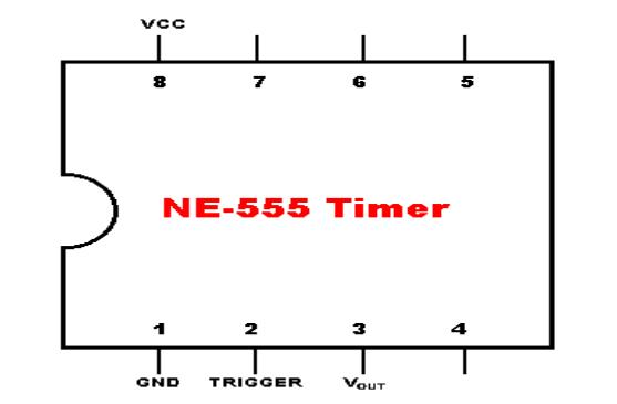
This is facilitated by the use of IC
NE-555, which generates series of output clock pulses. Actually, as shown
in the diagram the resistors and capacitors surrounding it formulate a
particular RC time constant and the IC then continues to generate output clock
pulses till the end of this time period. So, when the appropriate clock pulse
is obtained via the previously discussed circuit, the pulses generated by NE-555 are fed to the next IC-7493 i.e. Binary Ripple Counter (IC 7490 i.e. Decade Counter can also be used.) which counts from 0 to 7 i.e.
3-bit numbers (provided the MSB of the counter is not considered). When many
clock pulses are received by it in a single time-constant period, it counts
from 0-7 many times and outputs any of these numbers. This is seen as random
number generation.
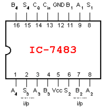
However, the numbers obtained from the above procedure are between 0
and 7 (inclusive), whereas numbers from 1-6 are only desired. This is taken
into account by the succeeding IC-7483
(Binary Parallel Adder) which increments the above generated number if it
is between 0 and 5, else Resets the Counter IC-7493
so that it outputs 0, which is then incremented to 1 by the Adder. The output
of the Adder is the final desired random number that can be fed into the
Dice-Display circuit.
|
Q |
Pulse |
|
000 |
0 |
|
001 |
1 |
|
010 |
2 |
|
011 |
3 |
|
100 |
4 |
|
101 |
5 |
|
110 |
6 |
|
111 |
0 |
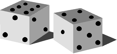
3. Dice-Displaying Circuit
The only purpose of this part is to show the face of the Dice
corresponding to the number generated by the randomizer circuit. This is done
by arranging 7 LEDS in the pattern as shown in the figure. Denoting each of the
LED by a particular name, the function of each LED can be worked out using
Boolean algebra. As previously discussed, a combination of AND, OR and NOT
gates provide the input to each LED grounded on the other end, so that the
desired LED glows when a number is generated.
The
display circuit is designed as per the following truth table:-
|
Count |
Q3 |
Q2 |
Q1 |
L1 |
L2 |
L3 |
L4 |
L5 |
L6 |
L7 |
|
|
|
|
|
Pattern of Glowing |
||||||
|
0 |
0 |
0 |
0 |
0 |
0 |
0 |
0 |
0 |
0 |
0 |
|
1 |
0 |
0 |
1 |
0 |
0 |
0 |
0 |
0 |
0 |
1 |
|
2 |
0 |
1 |
0 |
0 |
0 |
1 |
1 |
0 |
0 |
0 |
|
3 |
0 |
1 |
1 |
1 |
0 |
0 |
0 |
0 |
1 |
1 |
|
4 |
1 |
0 |
0 |
1 |
0 |
1 |
1 |
0 |
1 |
0 |
|
5 |
1 |
0 |
1 |
1 |
0 |
1 |
1 |
0 |
1 |
1 |
|
6 |
1 |
1 |
0 |
1 |
1 |
1 |
1 |
1 |
1 |
0 |
From
above table we
see that
L1= Q3 + Q1.Q2
![]() L2= Q3.Q2
L2= Q3.Q2
![]() L3= Q3 + Q2.Q1
L3= Q3 + Q2.Q1
L4= Q3 + Q2.Q1
L5= Q3.Q2
L6= Q3 + Q1.Q2
L7= Q1
4.
Adder Circuit
This is this core of this game. All numbers
generated so far must be accounted for each player independently in the form of
their score, which gets incremented by each alternate fall of numbers on the
dice. The Adder circuit does this. As shown in the figure, a group of 3 AND
gates commence the Adder. One of the inputs of the AND gates is a bit of the
random number and the other input is one of Q and Q’ (outputs of the J-K
flip-flop discussed in the ‘Clock Pulses’ section). Hence, at one time, the
score of the appropriate player gets incremented by the number on the dice,
whereas the score of the other player gets added by 0 (i.e. remains the same).
The outputs of the 3 AND gates enter the IC-7483 as input A having the MSB of A
grounded. The other input B comes from the output of the 4-bit Register IC-74194, which stores the LSB of the final score.
The output of this 1st IC-7483 is handed over to the 2nd
IC-7483, which converts the added binary number into its decimal equivalent and
stores the same in the above IC-74194 register. This conversion is done with
the help of AND and OR gates, as shown. When the binary number is greater than
9, 6 (0110) is added to it, thus generating the equivalent LSB decimal number,
else 0 (0000) is added to the number. In any case, the LSB remains less than or
equal to 9, thus representing the score in decimal form.
The same technique is applied to the MSB of
the score. For this 1 is added to the MSB IC-7483, if the above binary number
is greater than 9. The other input of this 3rd IC-7483 comes from
another 4-bit register IC-74194, so that MSB can also show decimal numbers from
0-9.
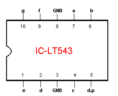
The same MSB and LSB numbers from the Adders
are given as input to IC-7448, which is the driver IC to the FND Seven-Segment
LED display. The outputs of this IC are fed to FND LT-543, to show the corresponding numbers.
Note here that the same ‘common clock’ is given
to the above IC-74194 registers so
that they can output the stored numbers each time.
5. ‘Game – Over’ disabling circuit
Considering the game to be over, once the
score of any of the two players reaches/crosses 40, the second MSBs of the MSB
of the decimal score of both the players are input to the NOR gate as shown.
Thus, when any score reaches/crosses 40, the 2nd MSB becomes HIGH.
Thus NOR output becomes LOW, which is then ANDED with the clock-pulse to be
given to the J-K flip-flop. Thus, the J-K flip-flop does not receive any clock.
So, the ‘toggling’ stops, random number generation stops, Dice-display remains
unchanged, and the scores remain fixed. Thus, the game is then said to be over.
The winning player is identified by the tone of the buzzer/alarm, which is
having one end on the above 2nd MSB and the other end grounded.
6. Reset Switch
The function of this switch is to bring the
game back to start from any point of time. This is done with the help of the
following Combinational Circuit and a ‘Push-to-OFF’
switch. Such a switch has its 2 ends always connected, except when
presses/pushed. So, here one end of the switch is grounded. This makes the
clear inputs of all registers HIGH by default. The registers employ Active Low
Clear inputs, and so, when the switch is not pushed, HIGH clear is fed to the
registers via a NOT gate, as shown. Therefore, normal functioning of all the
registers is obtained. Also the output of the drawn OR gate then depends on the
output of the AND gate (the 2 inputs of the AND gate being the 2nd
MSB and 3rd MSB of the output of IC-7493 Counter).
When the switch is pressed, the connection of
its 2 ends gets broken, the Clear input to all registers becomes LOW via the
NOT gate (i.e. all registers are cleared). So, one of the inputs to the IC-7483
Adders become 0000. Also the input of the OR gate becomes HIGH, thereby
ignoring the 2nd input and thus providing HIGH output to the RO(1)
Clear input of IC-7493 Counter. Its 2nd Clear input RO(2)
being HIGH, the counter is Reset providing 0000 output. This is provided as the
other input of IC-7483 Adder. Thus, the Adder circuits display 00 in the FNDs.
Also, this 000 output is carried via the Incrementor IC-7483 (in such
situation, the input carry is also 0) to the Dice-display circuit which shows
‘All-LEDs-OFF’ condition.
Two
players can play the game and when either of the player reaches the maximum
score the corresponding beeper starts beeping showing that he has won the
game.. Both the clocks are then disabled,
and beeper would beep until the reset button is pressed. LED box is also disabled so that no more
random numbers appear on it.
Thus we have successfully implemented the game of “Digital Dice”.